Advanced Imaging Pro has an interesting article on Kodak’s latest developments in sensor manufacturing. This was found via Flickr, which alludes to the possibility of a PMOS sensor.
The new PMOS apparently a new take on CMOS pixels and how they work on a camera sensor. In the Kodak PMOS the underlying polarity of the silicon is reversed, so the absence of electrons is used to detect a signal. This works the opposite way that normal pixels work: which instead detects electrons that are generated when light interacts with the sensor surface.
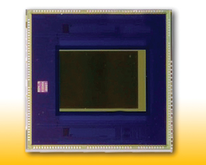
In addition to this, a new CCD sensor is being developed that, according to Samsung (as noted in the article), only uses 1/10th of the power that a regular CCD sensor uses: which means an insanely long battery life.
For current Olympus (and Panasonic) users, you can be glad to hear that the new sensors are focused on low-light photography, speed and HD video capabilities. However, we can still only just wait to see the results. When the Live MOS sensor was released it promised better low-light capabilities. In truth, it couldn’t match the capabilities of Canon or Nikon. Further, that isn’t a totally fair statement because of the fact that the sensor is smaller in size.
The new PMOS sensor could be what we see in the higher end pro camera models.


Not really sure why this would be lower power, certainly not 10x lower based on the fact that it is PMOS. CMOS is PMOS + NMOS hence C or complementary. The only difference between the two is that as you try to allude to that PMOS uses holes as the majority carriers in the device, which have a lower mobility. This means that the resistance of the device of equal size would increase. If you wanted a larger resistance for some reason than that might be a good thing. However, you are going to create electron hole pairs, not just holes and Johnson noise goes up with resistance, still we might be in shot noise dominated transport (actually that probably is the case, but I’d have to check), in which case maybe the trade of is okay. In any case, the difference in mobility is less than a factor of 2 so all the properties that would be affected would change by less than 2, certainly not 10. If they get 10 other things are going on.
Brian…
The 10X reduction in power stated in the article is not from the new PMOS sensor, but rather the CCD sensor that Samsung is developing.
You got your EE all wound up thinking you could impress everyone with your knowledge, but in the end, you couldn’t even read the article straight.
Get back to designing chips. LOL
Stewie don’t know if you are trying to go out of your way to be insulting… I see what you mean on careful reading, though I should think this one is more down to unclear writing. If you want to talk about more than one thing, it probably should be in the title. I skipped over “In addition to this” in the first reading I guess and thought that Samsung was being licensed to make the PMOS for Kodak. I don’t think Kodak has any major FABs.
Stewie & Brian? What is this an episode of Family Guy?